| PCB Design with TINA
Create single, double-sided or multilayer PCBs of your circuits with a single mouse click, using automatically-placed and routed components. All components in TINA are "PCB-ready" and have associated footprints. If necessary, you can review and edit a component's footprint using the components' spreadsheet. TINA's unique 3D capability displays a schematic with the physical parts in place of their electronic symbols. You can also view the PCB in 3D from any angle to see how it will look after manufacture.
The fully integrated layout module of TINA 7 has all the features you need for advanced PCB design, including powerful autoplacement & autorouting, manual and "follow-me" trace placement, DRC, forward/back annotation, pin/gate swapping, keep-in/out areas, thermal relief, fanout, plane layers, Gerber file output and much more.
Single layer SMD circuit
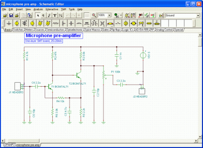
Schemaric diagram
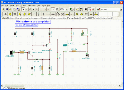
Schematic with 3D view of parts
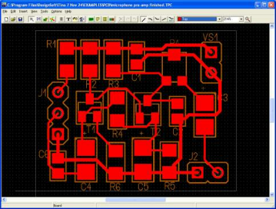
Single sided layout
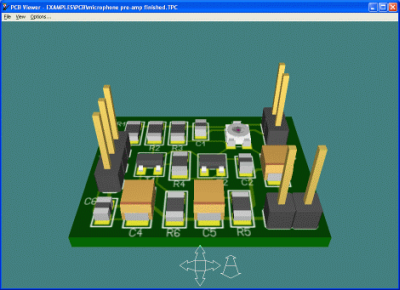
3D view of the circuit
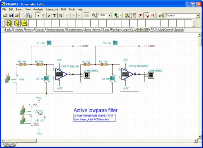
Double layer through-hole circuit
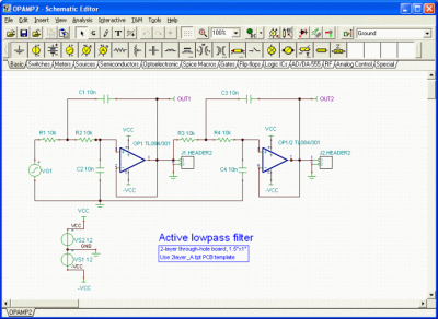
Schematic diagram of a double-sided design
3D part preview on the schematic
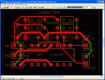
PCB layout with Top (red) layer selected
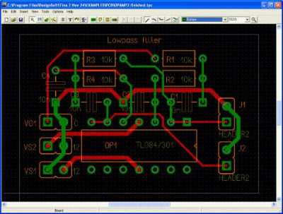
PCB layout with Bottom (green) layer selected
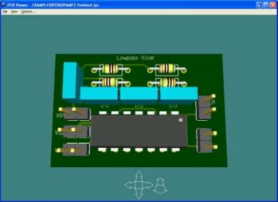
3D view of the top side
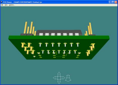
Looking at the bottom layer
4-layer SMD circuit
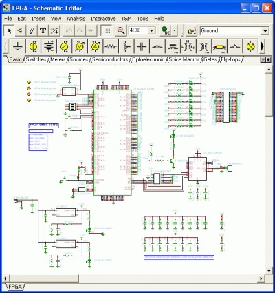
Schematic diagram of the 4-layer SMD design
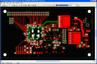
PCB layout of the 4-layer SMD design
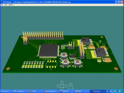
3D view of the top side
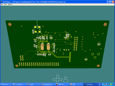
3D view of the bottom side
|


